Abstracts of the papers, as well as well as short biographical notes of the authors
Forum I, 6th of November, 2018
Session I A (9.10 a.m.-10.30 a.m.)
- IONUT RADU, Parc Technologique des Fontaines, 38190 Bernin, France, Material physics and technologies for substrate engineering to address challenges of semiconductor nanotechnologies, Soitec.
 |
Ionut Radu is Director of Advanced R&D at Soitec being responsible for research and development efforts in the field of advanced substrate technologies. Prior to being appointed to his current position, he held various technology management positions with responsibility in development of new substrate technologies for advanced electronic devices.
Dr. Radu obtained his B.S. in physics from University of Bucharest in 1999 and Ph.D (Dr. rer. nat.) in physics from Martin-Luther University Halle-Wittenberg in 2003. He has co-authored more than 70 papers in peer-reviewed journals, conference proceedings and reference handbooks and holds more than 40 patents in the field of semiconductor technologies. Dr. Radu is senior member of IEEE society and involved in Technical Program Committees of international conferences (ESSDERC, VLSI-TSA) and industrial forums (Semicon Europa). |
- MIRCEA DUSA, ASML Belgium, Kapeldreef 75, B–3001 Leuven, Belgium, Moore's Law and Optical Lithography Drive of Semiconductor Industry Progress.
 |
Mircea Dusa is a ASML Fellow and Staff Scientist with ASML. He is a founding member of ASML’s Technology Development Center working on exploratory imaging solutions for advanced lithography tools seeking integration of tool functionality and with non-litho tool components, the photomask, patterning processes and control metrology. Prior to ASML, Mircea held various engineering positions in semiconductor industry, both in R&D and manufacturing, at National Semiconductor/Fairchild Research Center, SEEQ Technology, Zygo Corporation in USA and at ICCE-IPRS in Romania.
He has published over 200 papers in the fields of lithography science and technology at various conferences and in referenced journals. He is a member of IEEE and a SPIE Fellow. He is an active member of SPIE, the International Society of Photo Instrumentation Engineers chaired the Advanced Lithography Symposium between 2013-2016 and Optical Microlithography Conference between 2008-2011. |
From 2008 to today, Mircea is teaching SPIE’s course on MultiPatterning Principles and Applications.
Mircea Dusa graduated with MS in EE and Solid State Physics from Polytechnic University of Bucharest and holds a Ph. D Degree in Applied Optics from the same university. |
Abstract. Over the past 50 years, Moore’s Law embodied semiconductor manufacturing progress by setting up the device scaling objective, “The number of transistors on a chip doubles every two year”. As a result of making smaller devices everything gets better, device speed goes up, power consumption goes down, reliability improves, the cost of making chips goes down, all as a result of technology. Lithography accounts for more than 60% of the technology innovations driving Moore’s Law, through making smaller structures on larger chips. To meet scaling challenges, lithographic process obeys Rayleigh resolution formula, R=k1 and the information transfer characteristics of the lithography lenses in terms of the number of pixels per image, N = Aimage /(CDmin). As per Rayleigh equation, achieving resolution involves reduction of illumination wavelength, increase of lithography lens numerical aperture, NA, and reduction of k1 factor through, for example, double patterning technique. In a lithographic system, larger number of pixels per image was achieved by the invention of scanner exposure technique providing almost 2x larger image field compared to traditional stepper systems. The cost of making chips using today’s expensive exposure tool necessitates high throughput that is achieved in TWINSCAN exposure systems with dual wafer stages. This presentation surveys the key innovations in lithography, optical resolution and exposure tool platform throughout semiconductor device scaling proving its enabling role, We will illustrate the intimate interactions between lithography key parameters, critical dimension uniformity and overlay, on transistor electrical parameters in a SRAM bitcell device. Finally, we will introduce the lithography of the future, the Extreme Ultra Violet, EUV Lithography. and the information transfer characteristics of the lithography lenses in terms of the number of pixels per image, N = Aimage /(CDmin). As per Rayleigh equation, achieving resolution involves reduction of illumination wavelength, increase of lithography lens numerical aperture, NA, and reduction of k1 factor through, for example, double patterning technique. In a lithographic system, larger number of pixels per image was achieved by the invention of scanner exposure technique providing almost 2x larger image field compared to traditional stepper systems. The cost of making chips using today’s expensive exposure tool necessitates high throughput that is achieved in TWINSCAN exposure systems with dual wafer stages. This presentation surveys the key innovations in lithography, optical resolution and exposure tool platform throughout semiconductor device scaling proving its enabling role, We will illustrate the intimate interactions between lithography key parameters, critical dimension uniformity and overlay, on transistor electrical parameters in a SRAM bitcell device. Finally, we will introduce the lithography of the future, the Extreme Ultra Violet, EUV Lithography. |
- FLORIN UDREA, Cambridge University, Cambridge CB3 0FA, Challenges in power semiconductor devices: technologies of the future.
 |
Florin Udrea is a professor in semiconductor engineering and head of the High Voltage Microelectronics and Sensors Laboratory at University of Cambridge. He received his PhD degree in power devices from the University of Cambridge, Cambridge, UK, in 1995, his Master degree from University of Warwick, UK in 1992 and his BSc degree from University Politehnica of Bucharest, Romania in 1991. Since October 1998, Prof. Florin Udrea has been an academic with the Department of Engineering, University of Cambridge, UK. Between August 1998 and July 2003 he was an advanced EPSRC Research Fellow and prior to this, a College Fellow in Girton College, University of Cambridge. He is currently leading a research group in power semiconductor devices and solid-state sensors that has won an international reputation during the last 25 years. Prof. Udrea has published over 500 papers in journals and international conferences. He holds 100 patents with 20 more patent applications in power semiconductor devices and sensors. |
Prof. Florin Udrea founded five companies, Cambridge Semiconductor (Camsemi) in power ICs – sold to Power Integrations, Cambridge CMOS Sensors (CCS) in the field of smart sensors – sold to ams, Cambridge Microelectronics in Power Devices, Cambridge GaN Device in high voltage GaN technology and Flusso in Flow and temperature sensors.
Prof. Florin Udrea is a board director in Cambridge Enterprise.
For his ‘outstanding personal contribution to British Engineering’ he has been awarded the Silver Medal from the Royal Academy of Engineering in 2012. In 2018 he received the Nanosmat medal and the prestigious Mullard award from the Royal Society.
In 2015 Prof. Florin Udrea was elected a Fellow of Royal Academy of Engineering. |
Abstract. The power devices field has seen tremendous changes in the last decade. The traditional power MOSFET has been largely replaced by a new class of
power devices based on the Silicon Sueprjunction concept, while the
Insulated Gate Bipolar Transistors (IGBTs) are now fabricated on 12 inch
wafers and have access to the latest thin wafer/trench/fine dimension
technologies. However most of the innovation and flavor in the field comes from the emergence of Wide Band Gap semiconductors – and in
particular the Gallium Nitride and Silicon Carbide. Extensive research
is also carried out in single crystal Diamond and Gallium Oxide
materials. The market of power devices has reached $30M and the annual
growth in IGBTs and Superjunction has been around 10%. GaN and SiC are expected to reach annual growth rates of 30% in the next 3-5 years. This
talk will cover a range of semiconductor technologies and materials for power devices and give a comparison between different technologies andmaterials for diverse applications such as power supplies, EV/HEV
converters, photovoltaic converters, traction and HVDC transmission
lines. New Figures of Merit (FOMs) will be defined for the materials and technologies of power devices. The talk will end with an outline of the challenges for the power electronics future and a vision of different technologies for the next 10 years. |
- VIOREL BANU, D+T Microélectronica A.I.E., Campus UAB, 080193 Bellaterra-Barcelona, Catalunya, Spania, The wide band-gap semiconductors, a new trend of power semiconductor devices development.
 |
Viorel Banu received his M.Sc. degree in Microelectronics and Semiconductor Devices from Politehnica University of Bucharest, Romania in 1978. Since 1978 to 2005, he was with IPRS–Baneasa, Bucharest, as fabrication leader for high power thyristor's and diode's passivated structures. He was also charged with the device development and technology research of high–power devices (thyristors and diodes) and responsible for high vacuum technologies and PECVD deposition. In 1999, he was appointed as Leader of the Department of High Power Devices and Applications. In parallel with his main responsibilities, he worked from 2001 to 2007 as Associate Designer for Bi–CMOS analog–mixed integrated circuits with O2Micro–Ltd. Since June 2007 he joined the Group of Power Devices and Systems from IMB–CNM (CSIC) Barcelona as Technology Engineer for WBG semiconductors. Here he is dealing with research and characterization of silicon carbide (SiC) and gallium nitride (GaN) devices, new test methods conception, test instruments construction and also with the design of one of the first generation of integrated circuits on SiC. He has published more than 80 research papers. |
Abstract. The progresses in manufacturing high quality wide bandgap materials from the last decade enabled the presence on the market of a wide variety of SiC an GaN devices that start to replace the former silicon power devices in the new projects. However many issues remain to be solved in the future for this new generation of power devices on wide band-gap semiconductors. The presentation shows the response to the new challenges of the research group from the Laboratory Power Devices and Systems from IMB-CNM CSIC, Barcelona, Catalunya-Spain. Are briefly presented the development results for high voltage diodes, MOSFETs, JFETs, BJT, Integrated Circuits for smart power, development of some specific test instrumentation and some new test methods conception. The last but not the least, will be presented the successfully participation to the space mission BepiColombo to Mercury Planet, as supplier of high temperature diodes for solar panels. |
Session I B (11.00 a.m.-12.40 p.m.)
- MARIUS NEAG, Technical University, Cluj-Napoca, Romania, Systematic and optimized design of analog ICs.
 |
Marius Neag received the Electronic Engineer Diploma from the Technical University of Cluj-Napoca, Romania, in 1991 and was awarded the PhD degree by the University of Limerick, Ireland, in 1999.
After working several years in Ireland and the US as a senior designer of RF, analog and mixed-signal ICs he returned to the Technical University of Cluj-Napoca where he lectures on the design of RF, Analog and Mixed-Signal ICs, as an Associate Professor.
There he has helped setting the “Digitally-Enhanced RF & Analog Integrated Circuits” research group. Marius Neag is the author and co-author of over 100 scientific publications, 2 books and 2 international patents. |
- IOAN-LUCIAN PREJBEANU, CEA, CNRS, INAC-SPINTEC, Grenoble, France, Magnetoresistive random-access memory (MRAM) concepts for extended scalability and ultrafast switching, Univ.Grenoble Alpes.
 |
Ioan Lucian PREJBEANU has been conducting research on nanomagnetism and spintronics for 20 years. He holds a Physics degree from Babes Bolyai University in Cluj (Romania) and a PhD in Physics from Louis Pasteur University in Strasbourg on magnetic nanostructures.
He then joined SPINTEC in Grenoble, where he pioneered scientific work on thermally assisted MRAM. Based on this proof-of-principle of the scientific concepts, Crocus Technology was founded in 2006 to develop and commercialize thermally assisted MRAM technology. |
| Lucian Prejbeanu joined Crocus Technology mid-2006 as R&D director, where he made key contributions to the development and industrialization of thermally assisted MRAM for which he was awarded the SEE-IEEE Brillouin prize in 2012. In 2013, Lucian Prejbeanu returns to SPINTEC as deputy director and became executive director as of January 1st, 2016. He holds 44 international patents on magnetic memories and magnetic sensors and has authored more than 80 scientific publications and book chapters on nanomagnetism and spintronics. |
| Abstract. Spintronics (spin-based electronics) was kick-started by the discovery in 1988 of the Giant Magnetoresistance Effect by the teams of Albert Fert and Peter Grünberg who were awarded of the Nobel Prize in Physics in 2007. For several decades, the hard disk drive industry has been a driving force for research and development in magnetism. Several new areas of strong potential industrial development are currently emerging in spin-electronics (MRAM and logic-in-memory architectures), in sustained development (permanent magnets, energy harvesting…), and in biotechnology. MRAM (Magnetic Random Access Memory) is one of a number of new technologies aiming to become a “universal” memory device applicable to a wide variety of functions. MRAMs are expected to combine non-volatility, high speed, moderate power consumption, infinite endurance, and radiation hardness, all at moderate cost and be easy to embed in devices. However, spin-based devices are still in their nascent stages, particularly at the sub-20nm dimensions, and in order to realize their potential, there is a need to strengthen the technology maturity and for advances in circuit designs and innovative architectures. In this presentation, I will describe several MRAM technologies developed in the last years at Spintec. |
- ALEXANDRU MULLER, IMT Bucharest, Romania, Novel high performance sensors using SAW resonators constructed on GaN/Si and operating at GHz frequencies.
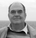 |
Alexandru Müller received his Ph.D degree in Semiconductor Physics from the University of Bucharest, in 1990.
He is the Head of the Microwave laboratory, in IMT–Bucharest, Romania. His early activity was focused on design and manufacturing of microwave diodes (pin, varactor step recovery, Schotttky). After 1995 he was involved in developing of novel membrane supported microwave and millimeter wave circuits based on micromachining technologies of silicon and GaAs. In the recent years his research activity was focused on acoustic devices developed on III Nitrides, analysis of Rayleigh and Sezawa propagation modes in GaN/Si layers. He has developed GHz operating SAW devices based on micromachinig and nanoprocesing of GaN/Si, targeting temperature and pressure sensor applications. |
He is the author/coauthor of more than 150 papers in high ranked journals and conferences. In 2003 he was invited “Directeur de recherché“ at LAAS CNRS Toulouse, France. He was involved in many European projects (in the frame of the research EU programs FP4, FP6, FP7, H2020) as coordinator or as resposible of the IMT team.
Dr. Müller has coordinated one of the first European projects in RF MEMS “MEMSWAVE” (1998–2001), nominated in 2002 between the 10 finalists for the Descartes Prize. He was awarded with the Tudor Tanasescu prize of the Romanian Academy in 2003 for the work: “Circuite microprelucrate pentru aplicatii in domeniul microundelor si undelor milimetrice – MEMSWAVE”, authors: A Muller, D Vasilache, S Iordanescu, D. Neculoiu, I Petrini, C Buiculescu, G Konstantinidis, F Giacomozzi. |
| Abstract. This work presents an overview of our recent results on the fabrication and characterization of GHz operating GaN/Si surface acoustic wave (SAW) resonators. Advanced micromachining and/or nanolitography processes have been used to manufacture high performance temperature and pressure sensors. GaN/Si SAW temperature sensors could be integrated in smart systems, able to monitor the temperature of power MMICs. Very novel possible applications of GaN/Si SAW structures are also presented. |
- ADRIAN IONESCU, EPFL Laussane, Elveția, Energy Efficient Electronics to Revolutionize Artificial Intelligence and its Applications.
 |
Adrian M. Ionescu is a Full Professor at Ecole Polytechnique Fédérale de Lausanne (EPFL), Switzerland. He received the BS & MS in Electronics and Telecommunications in 1989 from University ‘Politehnica’ Bucharest, Romania.
He holds two PhDs: in Microelectronics, from University ‘Politehnica’ Bucharest (1994) and in Physics of Semiconductor Devices from the National Polytechnic Institute Grenoble (1997). He is director of Nanoelectronic Devices Laboratory of EPFL, and he served as Director of Doctoral Program in Microsystems and Microelectronics of EPFL. He hold positions at CNRS and CEA-LETI, France. He was a visiting scholar at Stanford University, USA, and an invited Professor at Tokyo Institute of Technology, Japan.
His research group at EPFL pioneered energy efficient steep slope devices and novel MEMS active resonators, with emphasis on low power digital and analog/RF nanoelectronics. |
Prof. Ionescu published more than 600 articles. He is the recipient of IBM Faculty Award 2013 and of André Blondel Medal 2009, France. He also received the 2017 EDS George Smith Award. He served for 6 years as Editor of IEEE TED and as member of PUB committee of IEEE –EDS. Since 2015 he is member of Swiss Academy of Engineering Sciences (SATW). He is an IEEE Fellow and an ERC Advanced Grant awardee. |
- ANA RUSU, Royal Institute of Technology (KTH), Stockholm, Sweden, Future Smart Connected Society Enabled by Electronics.
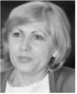 |
Ana Rusu received the M.Sc. degree in electronics and telecommunications from the Technical University of Iaşi, Iaşi, Romania, in 1983, and the Ph.D. degree from the Technical University of Cluj–Napoca, Cluj–Napoca, Romania, in 1998. She has been with the KTH Royal Institute of Technology, Stockholm, Sweden, since 2001, where she is currently a Professor of Electronic Circuits for Integrated Systems. Her research interests spans from low/ultra–low power high–performance CMOS circuits and systems for a wide range of applications, to emerging technologies, such as graphene, SiC, spin torque oscillators and M3D integration. |
Abstract. The continuous progress of semiconductor technology has a strong impact on our lives. The growing number of new applications (e.g. healthcare, autonomous vehicles and smart cities) and their very different requirements is creating new demands for semiconductor technologies, pushing the application-specific integrated circuits (ASICs) development in new directions. Technological innovation and novel approaches (e.g. Artificial Intelligence) are required for providing high degrees of sensing, processing, communication and heterogeneous integration capabilities as needed for a smart-connected society.
This presentation will share our state-of-the-art research results within bioelectronics, high-temperature electronics, M3D and STO technologies, which can enable the future smart-connected society and reshape our everyday life. |
Forum II, 7th of November, 2018
Session (8.30 a.m.-10.30 a.m.)
- MIHAI MIHAILA, IMT Bucharest, Romania, Microscopic origin of 1/f noise..
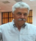 |
Mihai Mihaila holds a Ph. D. in physical electronics (1997, Politech. Univ. Bucharest). From 1971 till 1996 he was with ICCE - Bucharest, while from 1996 to 2003 he was a principal research scientist at National Inst. of Microtechnology (IMT). In 2003, he joined Honeywell Advanced Technology Center, Sensors Laboratory – Bucharest and left it in 2015 as senior principal research scientist. In 2015, he came back to IMT as a research scientist I. He is recognized for the discovery of the phonon resonances in 1/f noise and phonon fluctuation spectroscopy (US patent 7612551B1, 2009). He has more than 125 publications, 20 USA patents (23 pending), 5 EU patents, 1-Japan. Since 1999, he is a member (associate) of the Romanian Academy. |
Abstract. The evolution of the investigation on the origin of 1/f noise from the discovery of phonon resonances in it
till the recent first quantitative demonstration that electron-phonon coupling is its microscopic source will be presented. |
- SORIN MELINTE, Université catholique de Louvain, Belgium, Nanoarchitectonics with Si nanowires
 |
S. Melinte is Professor of Engineering in the Institute of Information and Communication Technologies, Electronics and Applied Mathematics at Université catholique de Louvain, Belgium. His current projects aim at developing novel nanodevices and hybrid inorganic-organic platforms for molecular electronics. In particular, his group uses high-resolution electron-beam nanolithography as well as soft-lithography and bottom-up nano- and micro-structuring techniques to engineer smart materials. |
Abstract. Nanoarchitectonics is a technology allowing the ordering of nanoscale structural units, which are usually a group of atoms or molecules, in an intended configuration. We’ll highlight nanoarchitectonics with Si nanowires. We’ll emphasize the importance of the metal assisted chemical etching method for the synthesis of advanced Si nanowires. One major research activity in nanoarchitectonics nowadays is centered on the anodes of Li-ion batteries built with Si nanowires. Silicon has been recently in the spotlight of the next generation anode materials for Li-ion battery industry due to its distinctive Li-related features such as the ability to form lithium rich compounds, corresponding to an exceptional capacity of 3579 mAh/g at low working voltages. We’ll discuss operational 3.4 V Li-polymer Si nanowire batteries, which are mechanically flexible and scalable to large dimensions and the key features of Si nanowires lithiation. |
- MIRCEA DRAGOMAN, IMT Bucharest , Romania, Nanoelectronics at the atomic scale: computing, harvesting, networking.
 |
Mircea Dragoman has graduated the Electronic Faculty, Polytechnical Institute in Bucharest, in 1980, and received the doctoral degree in electronics in 1991. During 1992–1994 he was the recipient of the Humboldt Fellowship award and has followed postdoctoral studies at Duisburg University, Germany. He was invited professor at: CNR– Istituto di Electtronica dello Stato Solido–Roma (1996), Univ. Saint–Etienne –France (1997), Univ. Mannheim (1998–1999, 2001–2002), Univ. Frankfurt (2003), Univ. Darmstadt (2004); in the period 2005–2006 he was nominated directeur de recherche at CNRS LAAS Toulouse. He had more than 40 invited papers in UE and two university courses in France (Nanoelectronics, 2005) and in Germany (Nonlinear Phenomena, 1992). |
He is Senior Researcher I with the National Research Institute for Microtechnologies. He co–authored more than 250 scientific papers and 6 monographies, such as M. Dragoman, D. Dragoman, Nanoelectronics. Principles and Devices,at Artech House, USA (2008)and M. Dragoman and D. Dragoman,2D Nanoelectronics, Physics and Devices of Atomically Thin Materials, at Springer (2017). Dr. Dragoman was awarded the Gheorghe Cartianu prize of the Romanian Academy in 1999. |
Abstract. The presentation is an overview of the recent results of the nanolelctronic devices based on atomically-thin materials (also termed as 2D materials) in computing, harvesting of electromagnetic energy and communications. The atomically-thick materials are considered to have a leading role in the future development of electronics. The Moore law has boosted half a century the main applications of electronics, but will attain soon many technological limits. As a result, new forms of computation such as quantum computing or neuromorphic computing are today searched and developed. Harvesting of the electromagnetic energy is the key concept for development of complex wireless networks which must be in principle battery-free. Also, the circuits of these complex networks must be tunable to respond quickly to various changes of ambient conditions. All these challenges regarding the future electronics trends during and post Moore law have promoted innovative devices based on various 2D materials such as graphene, ultrathin ferroelectrics, and semiconductor nanomembranes which will be analyzed during this talk. |
- SORIN CRISTOLOVEANU, MINATEC, Grenoble, Franța, The growing family of electrostatically-doped devices.
 |
Dr. Sorin Cristoloveanu received the PhD (1976) in Electronics and the French Doctorat ès-Sciences in Physics (1981) from Grenoble Polytechnic Institute, France. He is currently Director of Research CNRS. He served as the director of the LPCS Laboratory and the Center for Advanced Projects in Microelectronics, initial seed of Minatec center. He authored more than 1,100 technical journal papers and communications at international conferences (including 170 invited contributions).
He is the author or the editor of 36 books, and he has organized 35 international conferences.
His expertise is in the area of the electrical characterization and modeling of semiconductor materials and devices. He has supervised more than 100 PhD completions. He is the recipient of the IEEE Andy Grove award 2017. He is a Fellow of IEEE, a Fellow of the Electrochemical Society, and Editor of Solid-State Electronics. |
Abstract. The ‘electrostatic doping’ is a unique feature of nano-size structures: FD-SOI, nanowires, nanotubes, and 2D materials. In an ultrathin device, the electron/hole population induced by the gate spreads in the entire body (volume inversion or accumulation). This effect is very different from the charge-sheet interface layer formed in bulk semiconductors or in thick SOI. The physics, architecture and applications of most promising devices will be discussed.
The electrostatic doping enables to form junctions and contacts in technologies where physical doping is difficult (CNT, 2D, and NW devices). The body doping metamorphosis – from N to P or to ‘intrinsic’ – is also a fascinating tool for conceiving novel and reconfigurable devices. We show that devices with electrostatic doping offer unrivalled flexibility. For example, the band-modulation devices consist of successive N and P regions that are electrostatically doped to emulate a thyristor. Related applications are in the field of memory, electrostatic protection, sensing and fast logic.
An ultrathin extended drain MOSFET (LDMOSFET) with fully depleted drift region cannot drive current unless the virtual doping of the drain extension is tuned via a back gate. The operation of sharp-switching devices like tunneling FET (TFET) and I-MOS entirely relies on electrostatic doping. Another interesting device is the Hocus-Pocus diode which can be emulated in ultrathin SOI films by appropriately biasing the front and back gates. Adjacent electron and hole populations form a virtual P-N junction with multiple facets. |
- GHEORGHE BREZEANU, University Politehnica of Bucharest, Romania, Silicon Carbide for Sensing: a continuous challenge.
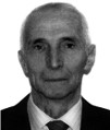 |
Gheorghe Brezeanu (M’90) received the M.Sc. and Ph.D. degrees in electronic engineering from the Electronic and Telecommunications Faculty of the University “Politehnica” of Bucharest, Bucharest, Romania, in 1972 and 1981, respectively. He has been with the same Faculty since 1972, focusing on the development of semiconductor devices and integrated circuits. In 1992 he became a Full Professor at the Department of Electrical Devices and Circuits, within the Electronic and Telecommunications Faculty, teaching “Electronic Devices”, ”Basic Electronic Circuits” and “Low–Power, Low–Voltage Analog ICs”. He was Scientific Chairman of the Faculty between 1996 and 2012 and since then he has been Director of the Ph.D. School. |
He is also Head of the Microsystems Master Program. His main area of research includes physics, modelling and fabrication of power and sensor devices on Si and SiC, and design and electrical characterization of low–power analog ICs. He founded the SiC Devices Group in the Advanced Power Semiconductor Devices Laboratory in 1995. This group was focused on research activities regarding design, fabrication and modelling of silicon carbide and diamond devices. He is the author or coauthor of 16 books and more than 230 papers published in technical journals and conference proceedings. He also holds five patents. Prof. Brezeanu was Chairman of the Electron Devices Society Romania Chapter from 1996 to 2008. He has also been an active member of the IEEE Electron Devices Society for over 20 years. |
Abstract. Silicon Carbide (SiC) is seen as a key material for hybrid and electric vehicles applications and high temperature, harsh environment-capable sensors. This wide gap semiconductor is suitable for sensors and power systems due to its higher breakdown electric field, high termal conductivity and current capability. In addition, it is a very hard material,chemically inert and highly resistant to radio-active environments.
This talk is focused on SiC sensor devices, capable of operating at high temperatures specific, for example to automotive applications. Temperature sensors based on forward biased SiC-Schottky diodes and SiC-MOS capacitor gas detectors are presented. Similar technologies, methods for extracting parameters and high temperature measurement techniques were developed for both detectors. Temperatures up to 450°C were accurately monitored. A peak responsivities to CH4 of 8.16% were determined with SiC gas sensors by investigations up to 200°C. |
- CORNEL COBIANU, IMT Bucharest, Romania, From thin films to nanosensor technology
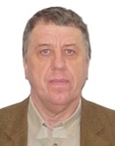 |
Dr. Cornel Cobianu. He is principal research scientist first degree at National Institute for Research and Development in Microtechnology -IMT Bucharest (since 2017), full member of Academy of Romanian Scientists (since 2012), co-founder of Honeywell Sensor Laboratory in Bucharest (2003), cofounder of the Center of Microtechnology Bucharest (1991), as well as Honeywell Fellow Engineering (2015).
Before joining Honeywell, he was full Professor of Electrical Engineering at "Valahia" University Targoviste and part-time Professor Researcher at University of Twente, The Netherlands.
During his work at Honeywell before 2017, Dr. Cobianu had a major contribution to the research and development of novel products and associated intellectual property.
Dr. Cobianu has been involved in EU-FP 4-7 programs being involved in projects like "PORSIS", e-CUBES", NEMSIC and recently in SOI-HITS project which received the innovation award above entire FP 7 competition.
|
| Dr. Cornel Cobianu has an extended experience in micro-nanoelectronics microsystem technology with focus on MEMS/NEMS chemical and physical sensors, where he has published 3 book chapters, 150 papers in journals and conference proceedings and was granted with 36 US Patents, 18 EU Patents, 4 CN Patents and 3 RO Patents, while more than 40 patents applications are pending, being cited more than 1300 times for his papers and patents. |
____________________________________________________________________________________________________
Back to EXCELNANO page____________________________________________________________________________________________________
ORGANIZERS.
European Excellence in Nanotechnology (EXCELNANO), Romanian Academy, Bucharest, 6-7 November 2018 is a combined event organized by the Romanian Academy, Commission for Science and Technology of Microsystems, www.link2nano.ro/acad/STMS, in partnership with the National Research and Development Institute for Microtechnologies (IMT Bucharest), Ministry for Research and Innovation, www.imt.ro
Media partners: Market Watch and Romanian Radio (Cultural branch).
|